


SiC³

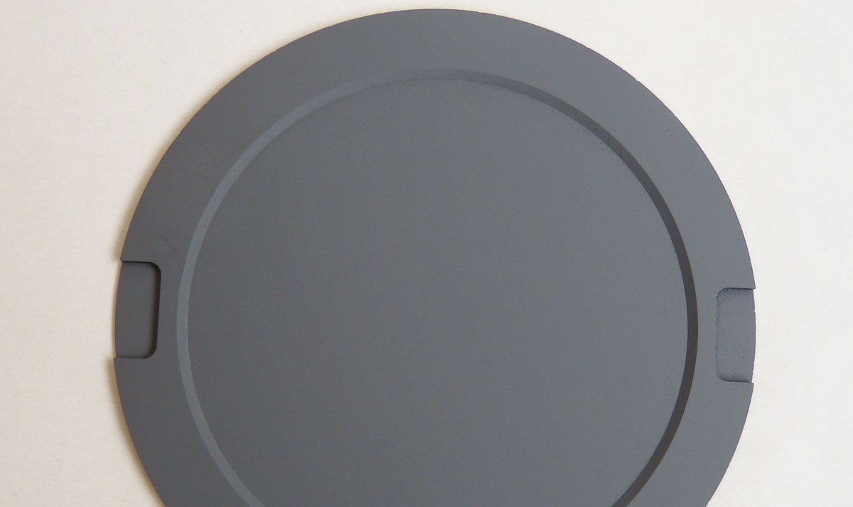
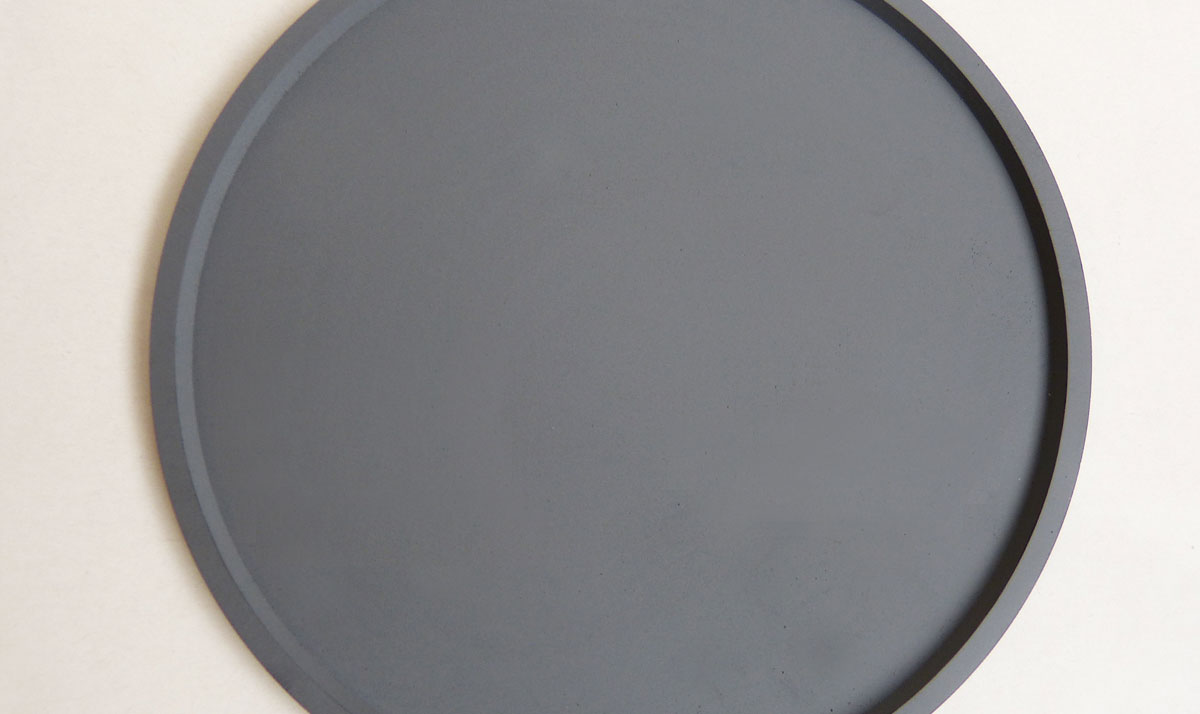


A New product to the mix - SiC³ Silicon Carbide Coated Parts
Quartztec Europe has entered into partnership with Thermic Edge Limited to manufacture and supply Silicon Carbide Coated products to our customers.
The process is unique as it combines a well defined crystal size, isotopic structure and low surface roughness. The high growth rate achieved by SiC³ ensures that the product remains cost effective.
The coating can be used in MOCVD, Epi, LED and other semiconductor, aerospace and heating technologies. Providing high purity and impervious layer on graphite, porous ceramics and composites. Our strong relationships allow us to provide high purity graphite within our product, allowing for a top-quality part to be manufactured and supplied.
Key Features
| Up to ∅350 Chamber Capacity | Isotropic Cubic Structure |
| Capacity to coat down to ∅1mm holes | High Purity Levels |
| Bespoke Layer Thickness | Excellent Coating Conformity & Hole Coverage |
| Flexible Coating Specification | Adjustable Surface Finish |
General Properties
Below illustrate the typical properties for SiC³.
We can also work with you to customise these properties to deliver a unique, fit for purpose part.
SiC³ Specification
| Property | Value |
| Density | 3200 kg.m³ |
| Crystal Structure | 3C (cubic; β) |
| Porosity | 0% (helium leak tight) |
| Crystal Size | 1 – 5 µm |
| Visual Appearance | Grey, satin to dull |
| Thermal Expansion (RT -400°C) | 4.2 x 10ˉ⁶m.Kˉ¹ |
| Thermal Conductivity (@20°C) | 200 W.m ˉ¹.K ˉ¹ |
| Elastic Modulus | 450 GPa |
| Electrical Resistivity(@20°C) | IMΩ.m |
| Element | Impurities (ppm) |
| Sodium | < 0.01 |
| Magnesium | < 0.01 |
| Aluminium | < 0.02 |
| Potasium | < 0.5* (lowest limit of detection with this method) |
| Calcium | < 0.05 |
| Titanium | < 0.005 |
| Vanadium | < 0.005 |
| Chromium | < 0.3 |
| Iron | < 0.04 |
| Cobolt | < 0.05 |
| Nickel | < 0.05 |
| Molybdenum | < 0.05 |
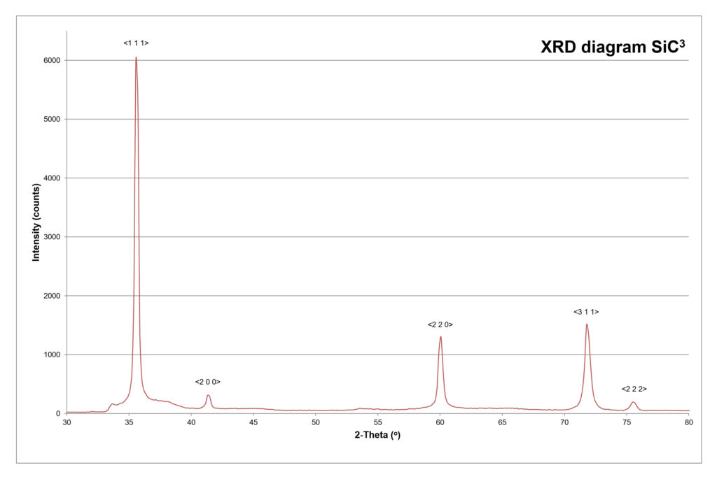
XRD
An XRD diagram is shown below. The peaks shown in the diagram perfectly match the 3C crystal structure.
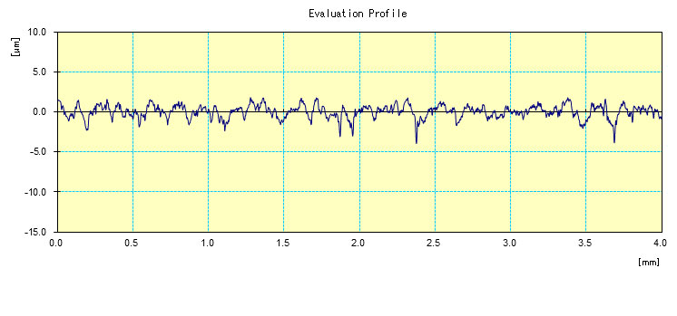
Surface Roughness
A typical surface roughness profile is shown below. The surface roughness parameters are Ra=0.8µm, Rz=5µm and Rt=8µm.
SEM
SEM Surface and Fracture analysis is shown in the following 2 images.
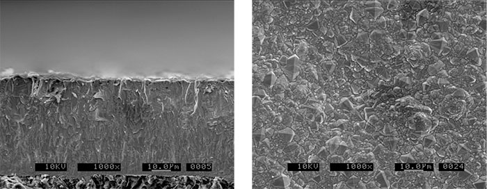
Surface analysis and Fracture Analysis
A huge advantage of SiC³ manufactured by CVD Technology, over line of sight process, is its “throwing power” or penetration depth. Hole diameters shown down to 1mm can be coated to a depth of 5mm, while still maintaining 30% layer thickness at its deepest point. Even more consistent layer thicknesses can be achieved when larger diameter holes are coated.
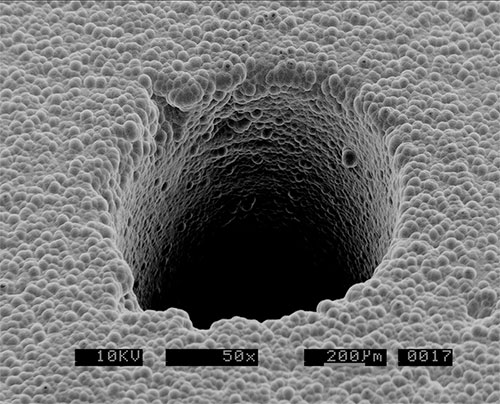
Covering Small holes